Preliminary Research of CZT Based PET System Development in KAERI
Article information
Abstract
Background:
For positron emission tomography (PET) application, cadmium zinc telluride (CZT) has been investigated by several institutes to replace detectors from a conventional system using photomultipliers or Silicon-photomultipliers (SiPMs). The spatial and energy resolution in using CZT can be superior to current scintillator-based state-of-the-art PET detectors. CZT has been under development for several years at the Korea Atomic Energy Research Institute (KAERI) to provide a high performance gamma ray detection, which needs a single crystallinity, a good uniformity, a high stopping power, and a wide band gap.
Materials and Methods:
Before applying our own grown CZT detectors in the prototype PET system, we investigated preliminary research with a developed discrete type data acquisition (DAQ) system for coincident events at 128 anode pixels and two common cathodes of two CZT detectors from Redlen. Each detector has a 19.4×19.4×6 mm3 volume size with a 2.2 mm anode pixel pitch. Discrete amplifiers consist of a preamplifier with a gain of 8 mV·fC-1 and noise of 55 equivalent noise charge (ENC), a CR-RC4 shaping amplifier with a 5 μs peak time, and an analog-to-digital converter (ADC) driver. The DAQ system has 65 mega-sample per second flash ADC, a self and external trigger, and a USB 3.0 interface.
Results and Discussion:
Characteristics such as the current-to-voltage curve, energy resolution, and electron mobility life-time products for CZT detectors are investigated. In addition, preliminary results of gamma ray imaging using 511 keV of a 22Na gamma ray source were obtained.
Conclusion:
In this study, the DAQ system with a CZT radiation sensor was successfully developed and a PET image was acquired by two sets of the developed DAQ system.
1. INTRODUCTION
In recent years, there has been growing interest in a compact and high performance positron emission tomography (PET) system for early diagnosis of diseases such as Alzheimer’s disease and cancer or for use in preclinical research. A conventional PET detector is based on a scintillator coupled with photo-sensors such as a photomultiplier or a silicon-photomultiplier (SiPM) [1]. Though the existing detectors, typically consisting of an LSO scintillator and PMT, have a good temporal resolution, relatively good efficiency, and low cost, these detectors have not only limited spatial resolution and energy resolution but are bulky in size due to full energy absorption of 511 keV annihilation photons [2]. Despite the semiconductor detector such as a high purity germanium (HPGe) detector having a very high performance for gamma ray detection, it always requires cooling to cryogenic temperatures for reducing the thermal noise [3]. Hence, room-temperature semiconductor radiation detectors (RTSDs), especially cadmium zinc telluride (CZT), are the most promising material for PET applications because of their high energy resolution, high spatial resolution, and relatively high detection efficiency compared to a scintillator [4, 5]. Since CZT also provides depth information of the interaction position using the signal difference between the cathode and anode, the parallax error which degrades the spatial resolution can be reduced [6].
In this study, we fabricated the CZT radiation sensor module and developed the data acquisition (DAQ) system for data acquisition from the signal of the CZT. For the evaluation of CZT crystal, the characteristics of CZT crystal such as electrical properties and energy resolution were performed. The amplifier modules were also developed for analog signal processing from CZT and evaluated with equivalent noise charge (ENC) and sensitivity. Finally, we obtained the PET image using a 22Na Gamma ray source, and the spatial resolution was measured.
2. MATERIALS AND METHODS
2.1 CZT radiation sensor module
Two 8x8 pixellated CZTs with a size of 19.4×19.4×6 mm3 from Redlen Tech. were used for radiation detection. Each CZT crystal was deposited with gold contacts at both cathode and 64 anode pixels. Because these CZTs cannot attach to the data acquisition (DAQ) system directly, the adapter board was developed considering a circuit line length avoiding a signal time-delay due to the position difference of each anode pixel. For bonding between CZT crystal and the adapter board, an indium ball and silver paste were used. Figure 1 shows the two CZT radiation sensor modules using pixellated CZT crystal and an adapter board. The characteristics of a CZT radiation sensor such as the current-to-voltage (I-V) curve, resistivity, and electron mobility life-time products were performed.
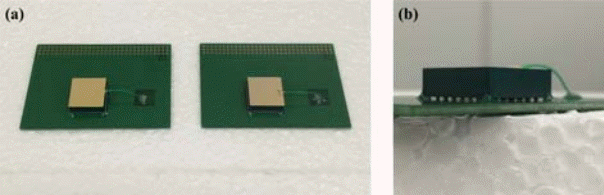
(a) Two sets of CZT radiation sensor bonded with adapter board. The indium ball and silver paste were used for bonding between CZT crystal and adapter board. (b) side view of CZT radiation sensor board. The indium balls which used for bonding between each pixel and adapter board can be identified.
2.2 Development of data acquisition (DAQ) system
When the ionization energy through radiation such as an X-ray or gamma ray is deposited to semiconductor radiation detector, then electron-hole pairs were generated. A charge-sensitive amplifier (CSA) converts the charges, which are proportional to radiation energy to voltage. Because the amplitude of a signal from the preamplifier is only a few millivolts, this voltage signal needs to be amplified and shaped. For previous analog signal processing, we developed a discrete-type ultra-low noise and highly sensitive amplifier module for room-temperature semiconductor radiation detectors based on the KAERI-PA preamplifier, which has ultra-low noise (~ 50 electrons) and high sensitivity (~ 7.2 mV·fC-1) at a low detector capacitance (< 1 nF). It is also composed of a CR-RC4 shaping amplifier and analog-to-digital convertor (ADC) driver, which makes two polarity (positive and negative) outputs in order to match with differential flash ADC for DAQ system. We also developed 64 + 1 channel DAQ system for digitizing an analog signal and data transfer. This system is composed of racks for the amplifier modules, nine differential flash ADC which has a 65 mega-sample per second sampling speed and 12-bit sampling resolution, field programmable gate array (FPGA) (Xilinx, San Jose, CA) with SDRAM, and a high-speed USB 3.0 module for reducing the data bottleneck when the data are transferred to a PC. Programmed FPGA was compatible for the ROOT (CERN, Geneva, Switzerland) code, and Anger logic was implemented for improving the spatial resolution. Figure 2 illustrates the two sets of DAQ systems with discrete-type amplifier modules and CZT radiation sensor modules.

64+1 channel DAQ system consists of rack of amplifier module, ADC, FPGA, and USB module.
2.3 PET image acquisition
A schematic diagram of the experiment is shown in Figure 3. A 22Na radioisotope, which emits a back-to-back gamma ray from the annihilation of positron, was used for PET imaging. The gamma ray source was positioned at the center of each CZT radiation sensor. The energy window was set between 495 keV and 526 keV. Images of the gamma ray source were reconstructed using 2-D filtered back-projection with a ramp filter.

Schematic diagram of an experiment geometry for acquiring PET image
3. Results and Discussion
3.1 Characteristics of CZT radiation sensor
Figure 4 shows I-V curves of the fabricated CZT radiation sensor with a bias voltage from -200 V and +200 V. The leakage currents with three different anode pixels (1 px., 10 px., and 50 px.) against an applied bias +200 V were 1.90 nA, 1.71 nA, and 1.37 nA, respectively. With measured I-V characteristics of the CZT radiation sensor, the average resistivity of the CZT radiation sensor were calculated as 4.02×10¹⁰ Ω·cm.
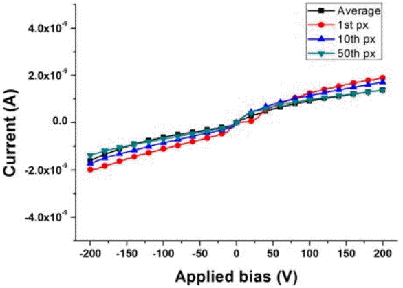
I-V characteristics with different pixel were acquired against bias voltage from -200 V to +200 V
For the electron mobility life-time products with a direct measurement method, we use events only occurring very close to the cathode, which have zero weighting potential [7]. The electron mobility life-time products were also measured and fractional electron loss per unit path length in a semiconductor, dN per dx, was characterized by
where λe is the mean free drift length of an electron. For the single polarity charge sensing technique, the signal amplitudes obtained from the anode pixels were proportional to the number of electrons. The number of electrons at drift length x can be defined as Equation 2.
where D is the detector thickness, N0 is the number of electron-hole pairs generated by incident radiation, and N1 and N2 are the measured photo-peak centroid channel numbers from the anode pixels at bias voltages V1 and V2 between the cathode and anode, respectively. From Equation 2, the electron mobility life-time products can be calculated directly as shown in Equation 3.
Based on a direct measurement method for the electron mobility life-time products with a 133Ba gamma ray source, we obtained the energy spectra with different bias voltages of 200 V and 500 V, as shown in Figure 5. The calculated mobility life-time product of the CZT radiation sensor was 2.76×10⁻² cm2·V-1.
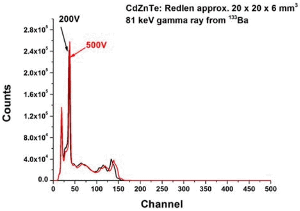
133Ba Gamma spectra versus bias voltage difference was used to calculate the life-time mobility products using direct measurement method.
3.2 Performance of the developed amplifier modules
For a performance evaluation of the developed amplifier modules, three characteristics such as ENC, sensitivity, and linearity were evaluated. ENC, which indicates the noise characteristics of the amplifier modules were calculated as follows:
The sensitivity, assumed to include all amplifying components such as the preamplifier, shaping amplifier, and ADC driver, was characterized by
We developed three amplifier modules based on a different preamplifier, and a shaping amplifier. Figure 6 shows the developed discrete-type amplifier modules with varying preamplifier and shaping amplifier. The version 1.0 amplifier module consists of a prototype preamplifier, which has an ENC of 100 electrons and sensitivity of 1 mV·fC-1. The version 2.1 amplifier module had a higher performance preamplifier compared with the version 1.0 amplifier module. Although the preamplifier of the version 2.2 amplifier module had the same ENC value as version 2.1, a higher sensitivity was achieved. The shaping amplifier in the version 2.2 amplifier module was also improved by a pole-zero cancellation and baseline correction. As shown in Figure 7, the version 2.2 amlifier module shows the best results in the ENC and sensitivity measurement. In addition, the amplitude linearity of the amplifier module as a function of the input energy shows a good linearity with a wide range of 0.1 to 1 MeV, as illustrated in Figure 8. When electronic noise in the amplifier module is to be minimized and the energy resolution enhanced, an optimized shaping time for the detector and small feedback capacitance of the preamplifier are needed for a better signal-to-noise ratio. The developed amplifier module can be modified by changing the CR value from 0.5 ns to 10 μs of peaking time and optimal shaping time was obtained for acquiring the PET image. In spite of the advantages of maintenances using a discrete-type amplifier module, it needs to improve on the bulky size and thermal control.

The developed discrete-type ultra-low noise and highly sensitive amplifier modules (a) ver. 1.0 consists of a prototype preamplifier, CR-RC4 shaping amplifier, and ADC driver (b) ver. 2.1 has higher performance of the preamplifier comparing to ver. 1.0 (c) ver. 2.2 was developed using the preamplifier which has lower ENC and higher sensitivity comparing to ver. 2.1 and modified shaping amplifier with pole-zero cancellation and baseline correction

Measured electric characteristics of ENC and sensitivity with amplifier modules. Version 2.2 amplifier module shows the best performance.
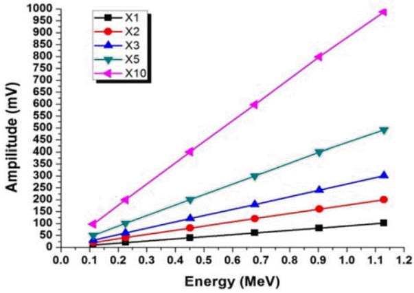
Amplitude linearity of the version 2.2 amplifier module as a function of input energy for a Si-PIN detector (W-value is 3.62 eV)
3.3 PET image acquisition
To calibrate the ADC channel of the system with the energy, the spectra of 22Na and 137Cs were acquired as shown in Figure 9. An average energy resolution of the anode pixels was 3.75% at 511 keV of the photo-peak energy of 22Na. Because of the high detection efficiency of the CZT radiation sensor, although the thickness of the CZT crystal is only 6 mm, the sum peak of 1.022 MeV of 22Na can be acquired. An average energy resolution of 3.73% was obtained for the 662 keV photo-peak energy of 137Cs. Because the channel numbers are proportional to the energy of the gamma ray, the ADC channel scale can be converted into an energy scale using a linear equation. After calibrating each anode pixel, we obtained the PET image using the developed system and two CZT radiation sensors. Figure 10 shows the reconstructed image using a filtered back projection with a ramp filter and the center profile. The spatial resolution, defined as the full width at half maximum (FWHM) of the point profile, was calculated as 3.07 mm. Because the CZT crystal has a relatively big anode pixel size and small area of the bulk CZT, the performance of the system, which means the spatial resolution and sensitivity are limited. The performance of the developed system can be improved using a smaller anode pixel size and thinner coincidence time window for reducing random coincidence events.
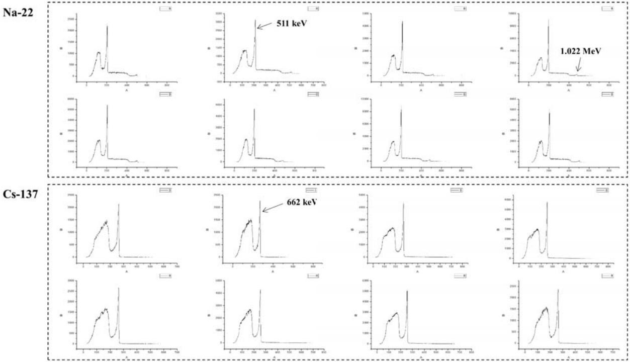
(a) 16 spectra from different anode pixels using 22Na radioisotope. 511 keV photo-peak and 1.022 MeV sum peak of 22Na can be identified. The average energy resolution of each anode pixel was 3.75% at 511 keV (b) 133Ba spectra from 16 anode pixels were obtained. The average energy resolution of each anode pixel was 3.73% at 662 keV.

(a) An acquired PET image and (b) a profile of acquired PET image.
4. CONCLUSION
In this study, the DAQ system with a CZT radiation sensor was successfully developed and a PET image was acquired by two sets of the developed DAQ system. The characteristics of the CZT radiation sensor were also evaluated by the I-V curve and the electron mobility life-time products. The developed system can achieve an energy resolution at 511 keV of 3.75% without any cooling system, and the spatial resolution of the acquired PET image was 3.07 mm. Because the developed DAQ systems are compatible with a discrete-type amplifier module, it is easy to conduct maintenance of analog devices such as preamplifiers or amplifiers. The programmed FPGA is not only compatible with the ROOT code, which based on C++, but can be easily modified for various applications such as a gamma camera, Compton camera, and SPECT. Although it has good strength for discrete-type amplifier modules, the bulky size owing to the arrangement of amplifier modules and the thermal problem are not negligible. We then tried to improve the application specific integrated circuit (ASIC) for replacing discrete-type amplifier modules and achieving a higher spatial resolution through an increase in the number of anode pixels. As mentioned above, we plan to experiment using CZT crystal, which has a much smaller anode pixel size for achieving a higher spatial resolution, and multiple CZT radiation sensor modules for covering a full field-of-view.
Acknowledgements
This work was financially supported by Nuclear R&D program of the Ministry of Science, ICT & Future Planning (MSIP) of South Korea (NRF-2010-0026096, NRF-2013M2A2A4023359, NRF-2013M2B2B1075775) and by a grant from Korea Atomic Energy Research Institute (grant No.:523280-16).