Effects of Fast Neutron Irradiation on Switching of Silicon Bipolar Junction Transistor
Article information
Abstract
Background
When bipolar junction transistors (BJTs) are used as switches, their switching characteristics can be deteriorated because the recombination time of the minority carriers is long during turn-off transient. When BJTs operate as low frequency switches, the power dissipation in the on-state is large. However, when BJTs operate as high frequency switches, the power dissipation during switching transients increases rapidly.
Materials and Methods
When silicon (Si) BJTs are irradiated by fast neutrons, defects occur in the Si bulk, shortening the lifetime of the minority carriers. Fast neutron irradiation mainly creates displacement damage in the Si bulk rather than a total ionization dose effect. Defects caused by fast neutron irradiation shorten the lifetime of minority carriers of BJTs. Furthermore, these defects change the switching characteristics of BJTs.
Results and Discussion
In this study, experimental results on the switching characteristics of a pnp Si BJT before and after fast neutron irradiation are presented. The results show that the switching characteristics are improved by fast neutron irradiation, but power dissipation in the on-state is large when the fast neutrons are irradiated excessively.
Conclusion
The switching characteristics of a pnp Si BJT were improved by fast neutron irradiation.
Introduction
Bipolar junction transistors (BJTs) are widely used as amplifiers and switching devices. When BJTs are used as switches, they have a long turn-off time (toff) because the lifetime of minority carriers is long [1]. It is thus difficult to use BJTs as high frequency switching devices. When BJTs operate as low frequency switching devices, the power dissipation in the on-state is large. On the other hand, when they operate as high frequency switching devices, the power dissipation during the switching transient increases rapidly. The lifetime of BJTs can be shortened due to repeated abrupt power dissipation during the switching operation.
To use BJTs as high frequency switching devices, several methods that increase the recombination of minority carriers during turn-off transient by shortening the lifetime of minority carriers are being employed. The thermal diffusion method and the high energy particle irradiation method are generally used to shorten the minority carrier lifetime. Platinum is typically used in the thermal diffusion method [1]. However, it is difficult to obtain precise performance with the thermal diffusion method because this approach is greatly affected by temperature during the manufacturing process. In high energy particles irradiation, gamma rays, electron beams, protons, and neutrons are used [2–7]. Irradiation by high energy particles causes total ionization dose effect and displacement damage [8, 9]. The total ionization dose effect occurs when energy particles collide with atomic electrons, and mainly affects the silicon dioxide (SiO2) and silicon (Si)-SiO2 interface regions of the BJT. Displacement damage meanwhile creates defects inside the Si bulk. Fast neutron irradiation mainly results in displacement damage rather than a total ionization dose effect [9]. Therefore, fast neutron irradiation has the advantage of effectively generating defects in the Si bulk [10–15]. The lifetime of minority carriers is shortened because the defects act as recombination centers for minority carriers. In this study, experimental results on the switching characteristics of a pnp Si BJT such as the switching time, voltage and current, and power dissipation during switching before and after fast neutron irradiation are presented.
Materials and Methods
1. Switching Characteristics of BJT
BJT switch circuits are composed of circuits that control the collector voltage (vc) and collector current (ic) by changing the base voltage (vb). In a pnp BJT, the vb is applied as a negative voltage to turn-on the BJT from the off-state to the on-state. The vb is applied as 0 V or positive voltage to turn-off from the on-state to the off-state. Fig. 1 shows the changes in the vc and the ic for the variation vb during switching in the pnp BJT switching circuit [1, 16].
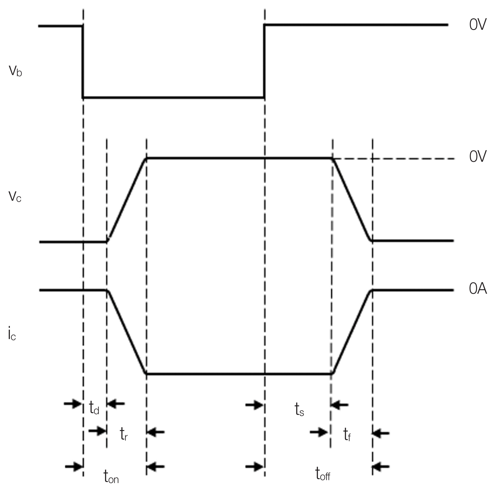
Switching characteristics of pnp bipolar junction transistor. Vb, base voltage; Vc, collector voltage; Ic, collector current; td, delay time; tr, rising time; ton, turn-on time; ts, storage time; tf, fall time; toff, turn-off time.
Turn-on time (ton) is composed of delay time (td), which is the time required for the ic to get out of the cut-off state, and rising time (tr), which is the time that it takes for the collector to reach saturation after leaving the cut-off state. toff is composed of storage time (ts), which is the time required for the ic to get out of the saturation state, and fall time (tf), which is the time that it takes for the ic to reach the off-state from saturation. ton, including td and tr, is insensitive to changes in the lifetime of the holes, which are the minority carriers in the base region. Meanwhile, ts and tf decrease as the lifetime of the holes decreases [17]. That is, toff decreases as the lifetime of the holes in the base decreases.
2. Fast Neutron Irradiation Effects
The pnp BJT switches operate in the operating state under the forward-biased emitter junction and the reverse-biased collector junction. Base current is composed of the current by electrons that recombine with holes in the base, the current by electrons injected from the base to the emitter, and the current by electrons generated at the collector caused by thermal generation and injected into the base [17]. The recombination current is dominant in the base current. ic is composed of the current generated by holes that are injected from the emitter to the base and then pass through the base and reach the collector, and the current by holes generated at base caused by thermal generation and injected into the collector. The dominant current of the ic is the current by holes started at the emitter and arriving at the collector. When energetic particles are irradiated onto semiconductor devices, the energy particles causes a total ionization dose effect and displacement damage [8, 9]. The total ionization dose effect occurs when energy particles collide with atomic electrons, and mainly affects the SiO2 and Si-SiO2 interface regions of the BJT. In addition, displacement damage creates defects inside the Si bulk. When fast neutrons are irradiated on Si BJTs, defects caused by displacement damages dominantly occur in the Si bulk rather than the total ionization dose effect [9]. The main changes of electrical properties in BJTs irradiated by fast neutrons are caused by defects inside the Si bulk. Vacancies and interstitial positions occur in Si lattice sites and act as defects [15, 18, 19]. These defects serve as recombination sites of carriers. Fast neutron irradiation of Si BJTs increases the recombination of minority carriers in the base, increases the base current, and decreases the ic. When BJTs are used as switching devices, the ton is hardly affected by the lifetime of the minority carriers, but the toff decreases as the lifetime of minority carriers decreases.
3. Experimental Setup
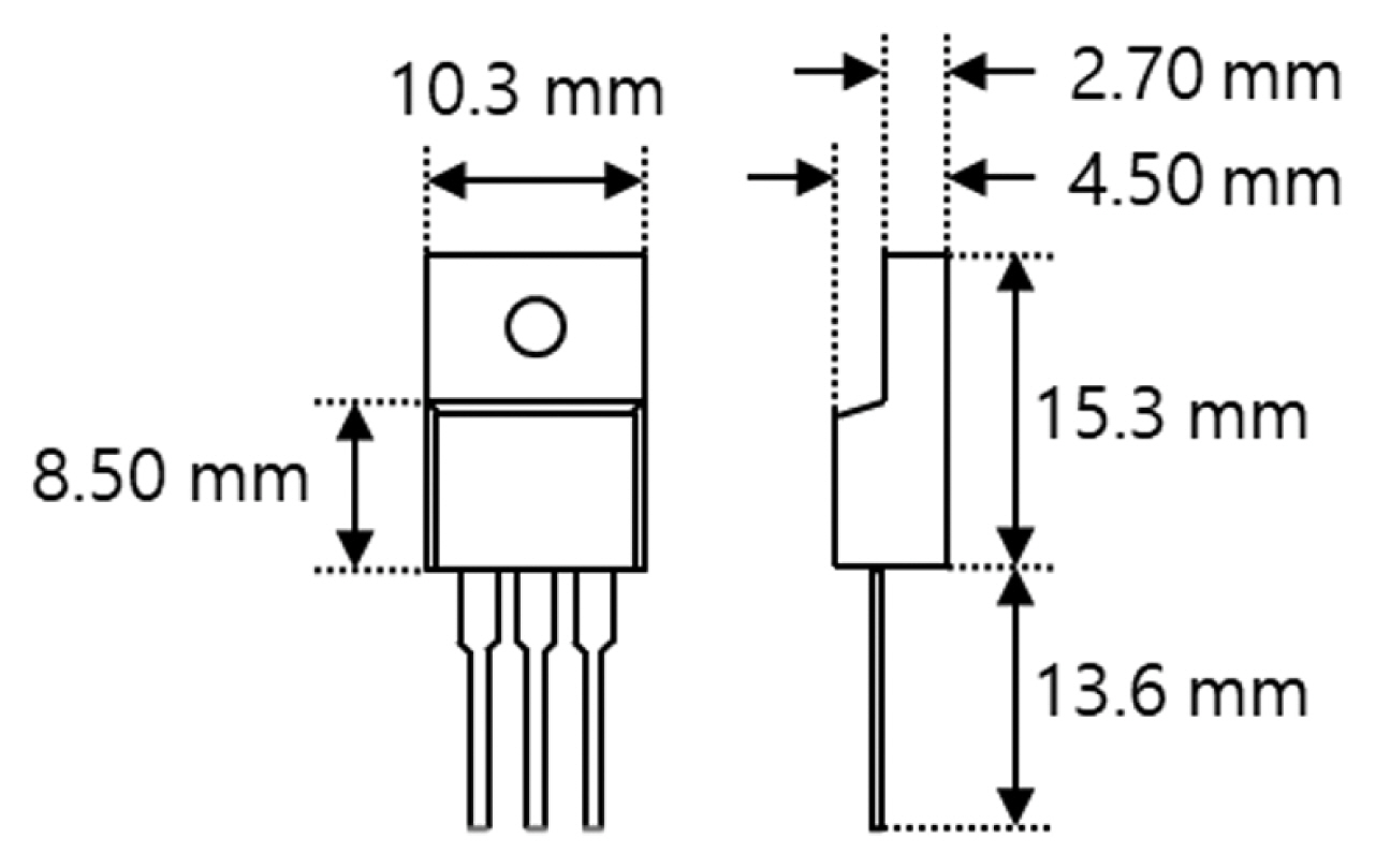
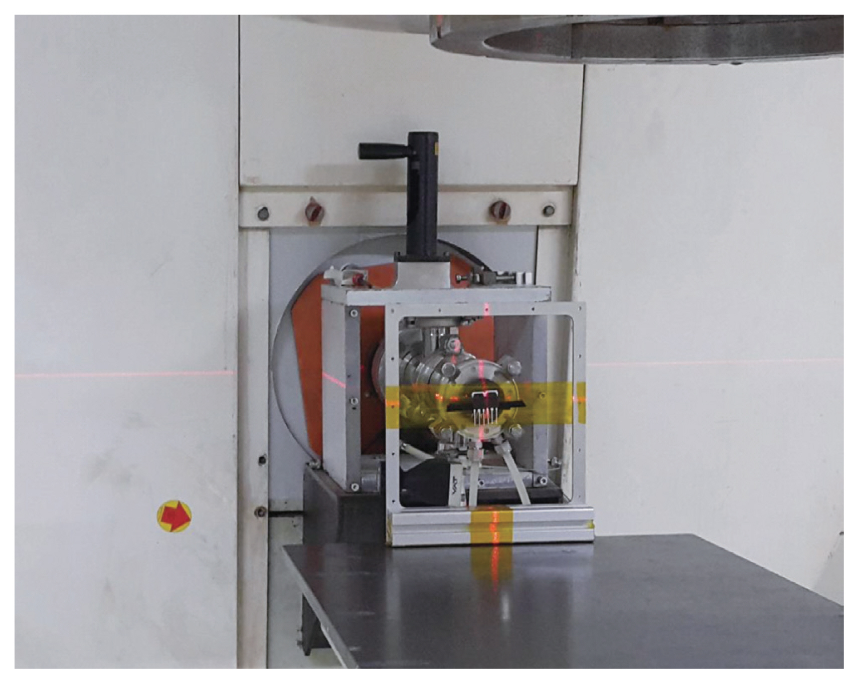
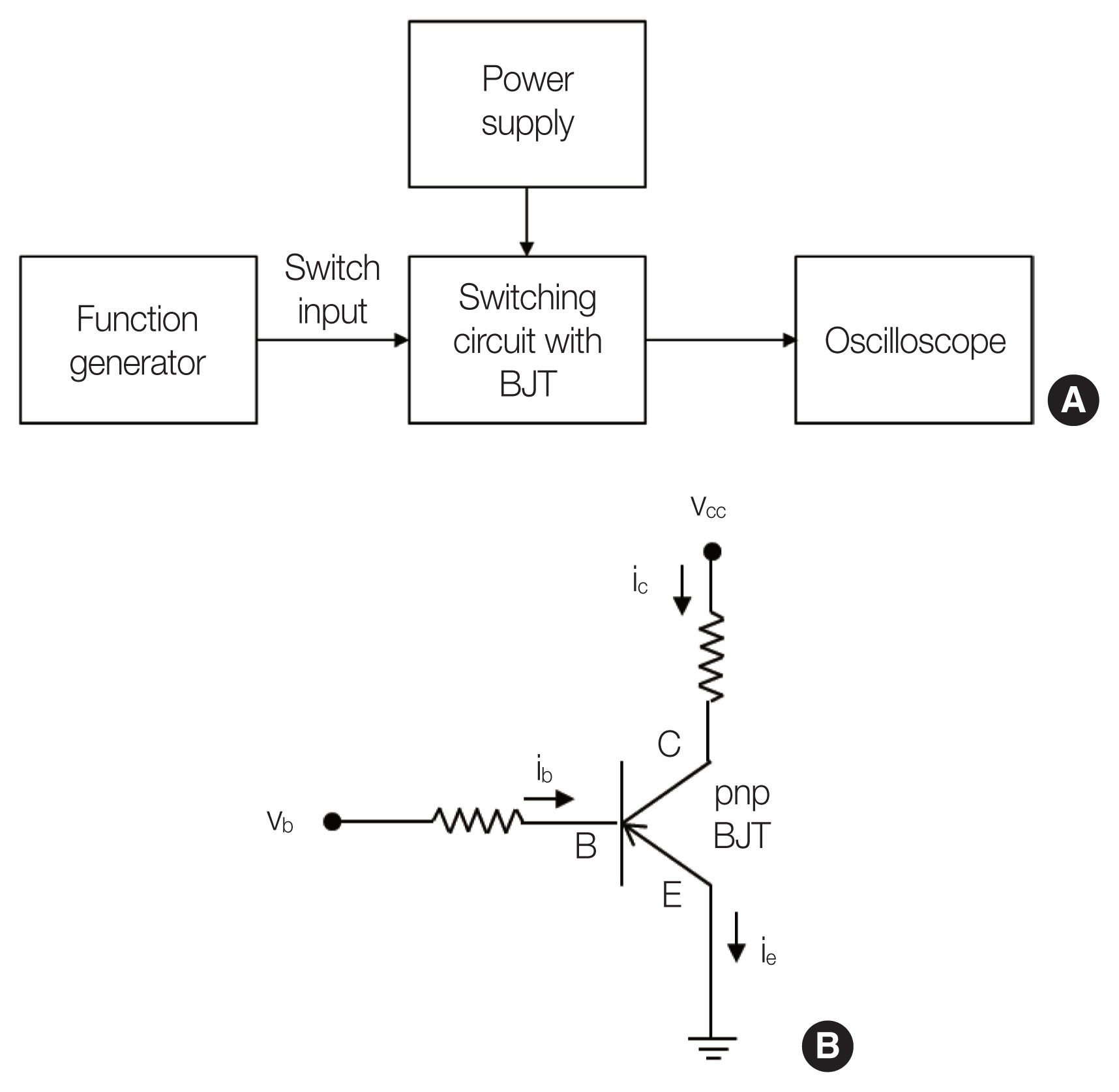
A pnp Si BJT in the form of a package generally employed in amplifiers or switching devices is used in the experiment. The configuration and ratings of the pnp Si BJT are given in Table 1, Fig. 2. The BJT was irradiated by fast neutrons generated from an MC-50 cyclotron in Korea Institute of Radiological & Medical Sciences. The fast neutrons were generated from a beryllium (Be) target with 30 MeV protons as shown in Fig. 3 [20]. In the MC-50 cyclotron, the angular distribution of neutrons are uniform when the angle from the Be target is less than five degrees [20]. Therefore, the irradiation samples were placed at an angle less than five degrees. The irradiated fast neutron fluences were 1×10⁹, 1×10¹⁰, 5×10¹⁰, and 1×10¹¹ neutrons/cm2. A Keithley I–V measurement device was used to measure the electrical characteristics of the BJTs. Fig. 4 shows the schematic diagram for measurement of switching characteristics. A common-emitter type switching circuit with a pnp BJT was used for the switching characteristics tests. An Agilent 33250A function generator, a GPS-2303 power supply (GW INSTEK), and a MDO3054 oscilloscope (Tektronix) were used.
Results and Discussion
1. Switching Characteristics
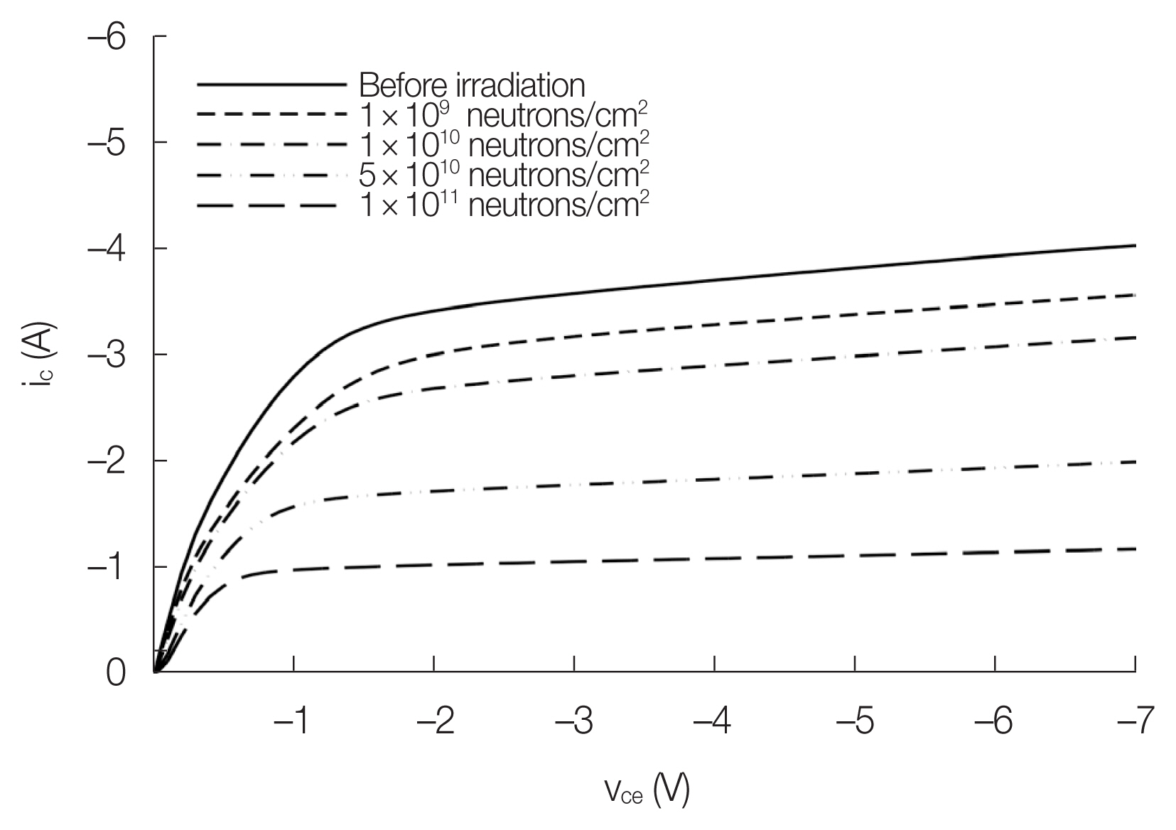
Fig. 5 shows the ic versus the collector-emitter voltage (vce) for fast neutron fluences. It shows that the ic decreases as the fast neutron irradiation increases. This indicates that the holes arriving at the collector are reduced as the recombination of holes increases in the base.
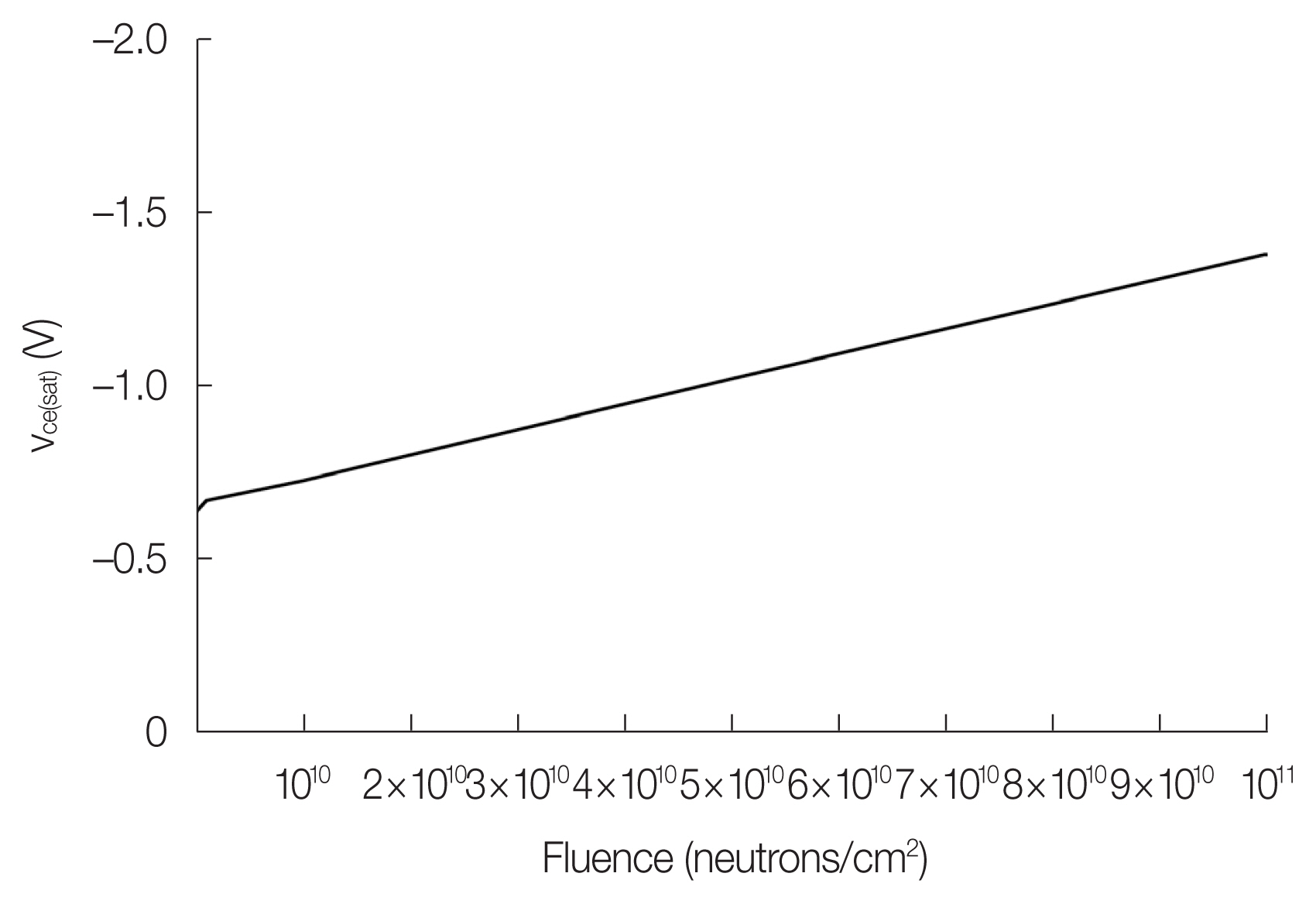
Fig. 6 shows the collector-emitter saturation voltage (vce(sat)) for fast neutron fluence. In the specifications of the pnp Si BJT used in the experiment, vce(sat) is defined as the vce value when the ic is −4 A and the vb is −0.4 A. It is shown that vce(sat) increases as the fast neutron irradiation increases.
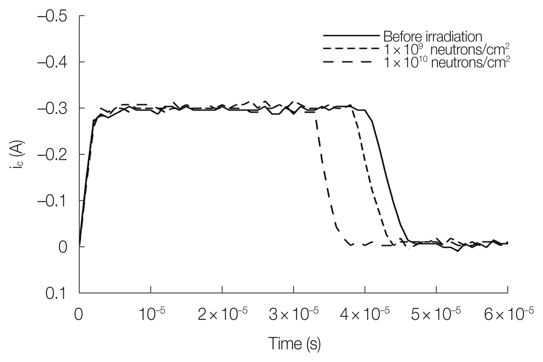
Figs. 7, 8 show the vc and the ic, respectively, during one switching cycle of the BJT including turn-on and turn-off. The irradiated fast neutron fluences were 1×10⁹ and 1×10¹⁰ neutrons/cm2. The BJT maintained the off-state before applying the input for turn-on to the vb. The input voltage to the vb was applied to the BJT switch maintaining off-state to turn-on at 0 second. In order to turn-off the BJT while maintaining the on-state, the base input voltage was changed to 0 V at 3×10⁻⁵ seconds. It can be seen in Fig. 7 that the vc in the on-state increases slightly as the fast neutron irradiation increases. This indicates that the vc increases due to an increase of resistance by an increase of defects caused by fast neutron irradiation. It is shown in Figs. 7 and 8 that the toff has a greater influence on the switching time delay than the ton. The ton slightly increases for the turn-on transient as the fast neutron irradiation increases. However, the increase in ton is negligible. This indicates that the ton is insensitive to the lifetime of minority carriers in the BJT. The toff decreases to 87.5% (in the case of 1×10⁹ neutrons/cm2) and 43.75% (in the case of 1×10¹⁰ neutrons/cm2) compared to before irradiation. This indicates that the defects increase in the Si bulk of the BJT with an increase of fast neutron irradiation and the toff decreases due to a decrease of the minority carrier lifetime by an increase of defects at the base during the turn-off transient. As a result, it can be seen that the switching time is improved by the fast neutron irradiation.
2. Power Dissipation
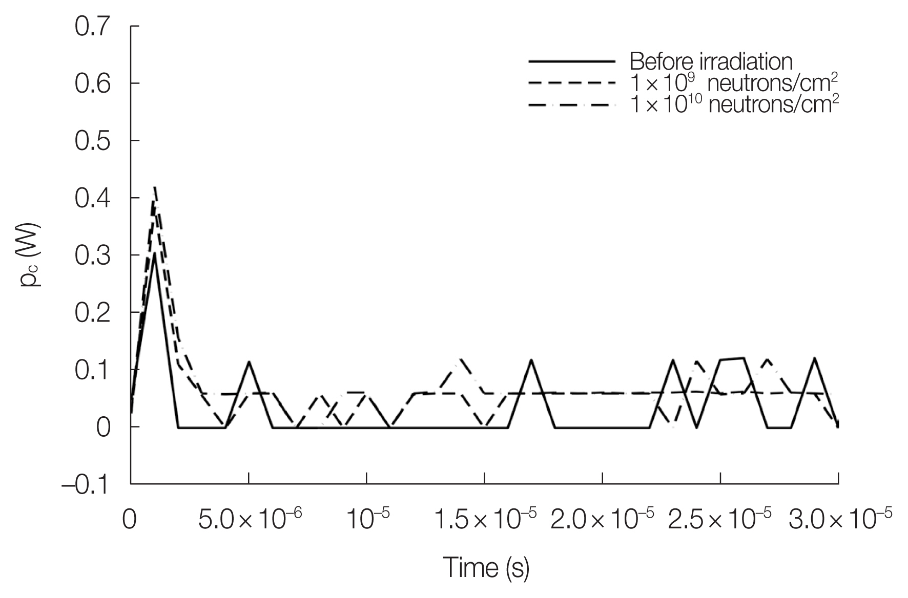
Fig. 9 shows the collector power dissipation (pc) upon fast neutron radiation during turn-on switching. This shows that the pc tends to slightly increase during the turn-on transient as the fast neutron irradiation increases, but the increase is very small. Furthermore, it can be seen that the pc in the on-state slightly increases as the fast neutron irradiation increases. This indicates that the pc increases in the on-state due to an increase of resistance by an increase of defects caused by irradiation of fast neutrons.
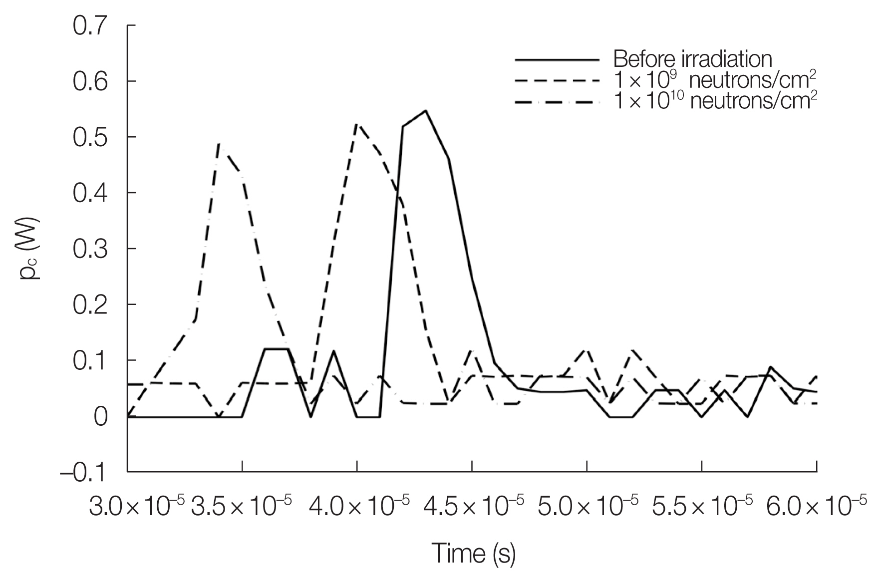
Fig. 10 shows the pc upon fast neutron irradiation during turn-off switching. This shows that the pc tends to decrease during the turn-off transient as the fast neutron irradiation increases. In addition, it can be seen that the pc time shifts forward because the toff decreases as the fast neutron irradiation increases.
3. Switching Characteristics upon Excessive Irradiation
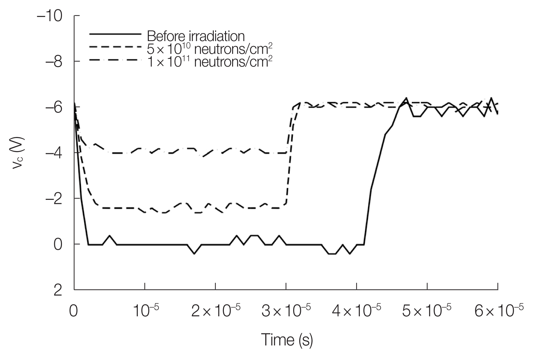
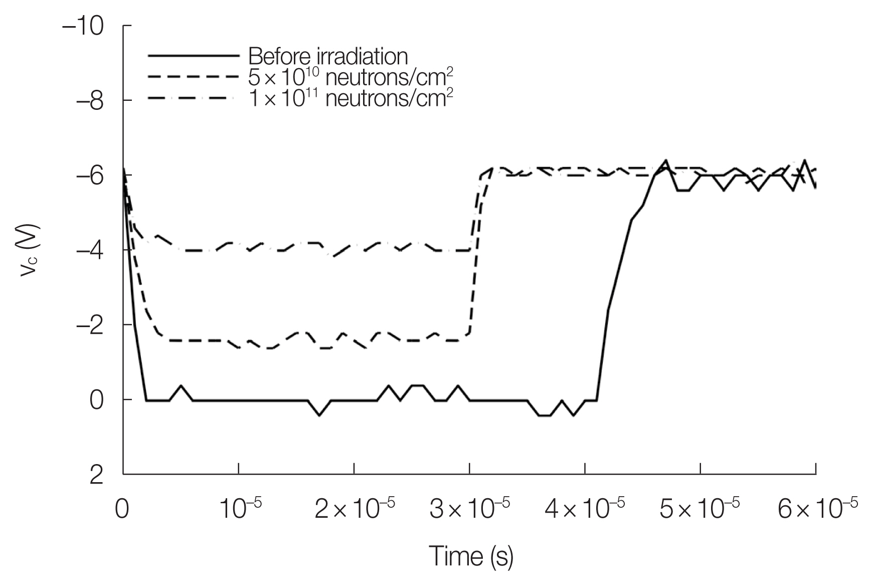
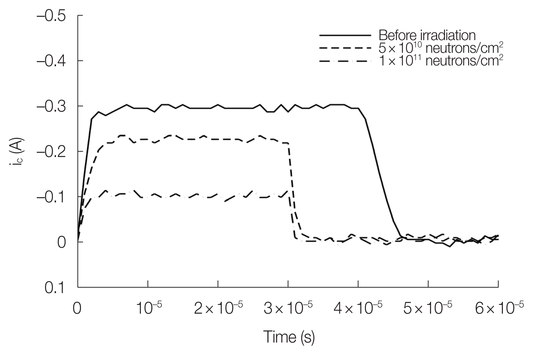
Figs. 11, 12 show the vc and ic, respectively, during one switching cycle of the BJT including turn-on and turn-off in the case of excessive irradiation of fast neutron. The irradiated fast neutron fluences on the BJTs were 5×10¹⁰ and 1×10¹¹ neutrons/cm2. The BJT maintained the off-state before applying the input for turn-on to the vb. The input voltage to the vb was applied to the BJT switch while maintaining off-state to turn-on at 0 second. In order to turn-off the BJT while maintaining the on-state, the base input voltage was changed to 0 V at 3×10⁻⁵ seconds. Figs. 11, 12 show that there are no significant changes in the ton as the fast neutron irradiation increases. However the ic decreases and the vc increases during the on-state as the fast neutron irradiation increases. This indicates that the voltage drop of the collector increased because the resistance significantly increased in the Si bulk due to increased defects caused by excessive irradiation. Also, these results show that the toff decreases greatly as the fast neutron irradiation increases.
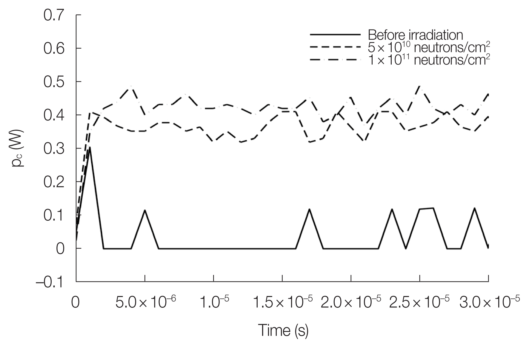
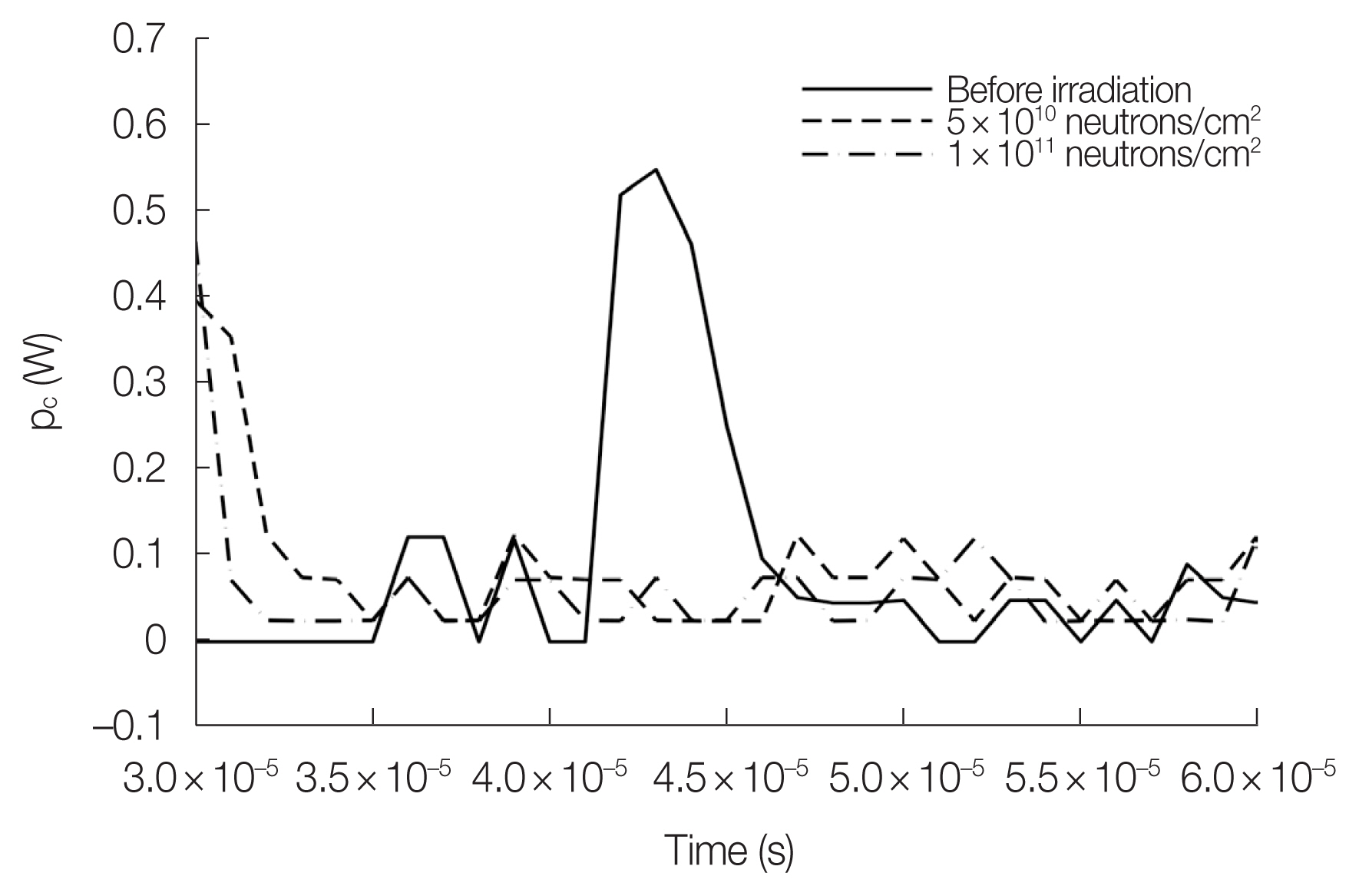
Figs. 13, 14 show the pc for turn-on switching and turn-off switching in the case of excessive irradiation of fast neutrons. It is shown that when the BJT is excessively irradiated with fast neutrons, the pc increases substantially during the on-state. This indicates that the power dissipation increased because the voltage drop of the collector significantly increased due to increased defects by excessive irradiation. Therefore, it can be seen that the switching performance is degraded in the case of excessive irradiation.
Conclusion
When BJTs are used in switching devices, there is a limitation of high frequency response characteristics because BJTs have long toff during switching. The power dissipation during the switching transient increases rapidly when BJTs operate as high frequency switching devices. The lifetime of BJTs can be shortened due to repeated abrupt power dissipation during the switching operation. Furthermore, the toff can be reduced by shortening the minority carrier lifetime of BJTs. When fast neutrons are irradiated on Si BJTs, defects by displacement damage mainly occur in the Si bulk rather than the total ionization dose effect affecting the SiO2 and Si-SiO2 interface regions. The lifetime of the minority carriers is reduced due to these defects, because the defects act as recombination sites of minority carriers in BJTs.
This study presented the experimental results for a pnp Si BJT upon variation of voltage, current, and power dissipation by fast neutron irradiation during switching. The results show that the toff decreases significantly and the ton slightly increases as fast neutron irradiation increases. The pc decreases during the turn-off transient as the fast neutron irradiation increases. In addition, the pc slightly increases during the turn-on transient and the on-state as fast neutron irradiation increases. However, with excessive irradiation of fast neutrons, the pc of for the pnp Si BJT increases significantly during the on-state. The switching performance can be degraded by excessive irradiation of fast neutrons. As a result, the switching characteristics of the pnp Si BJT can be improved in the high frequency region by appropriate fast neutron irradiation.
Notes
Conflict of Interest
No potential conflict of interest relevant to this article was reported.
Ethical Statement
This article does not contain any studies with human participants and animals performed by any of the authors.
Author Contribution
Conceptualization: all authors. Methodology: all authors. Formal analysis: all authors. Visualization: Ahn SH. Writing - original draft: Ahn SH. Writing - review and editing: Sun GM. Approval of final manuscript: all authors.
Acknowledgements
This work was supported by the Korea government (MSIT) (1711078081).


